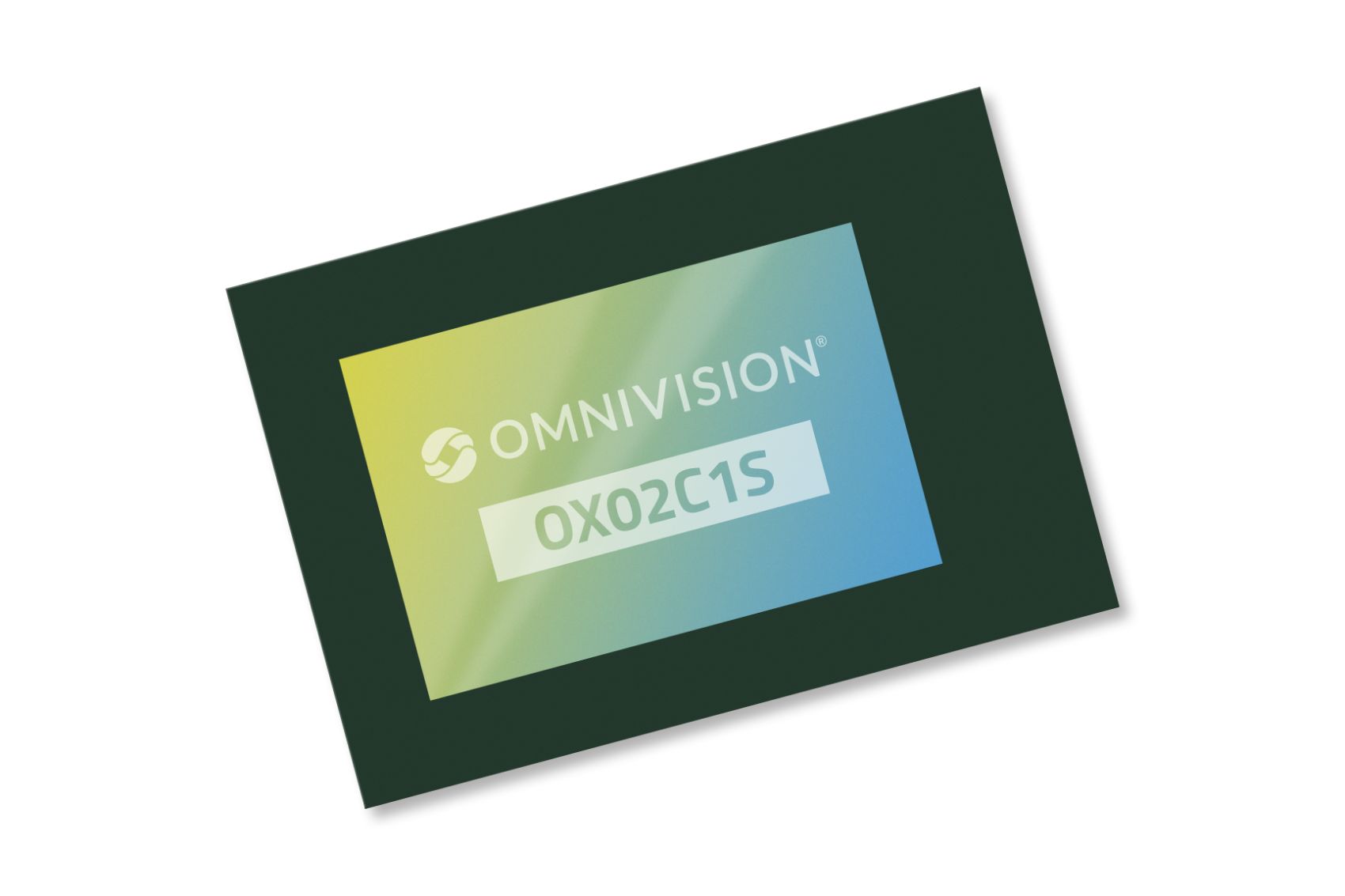
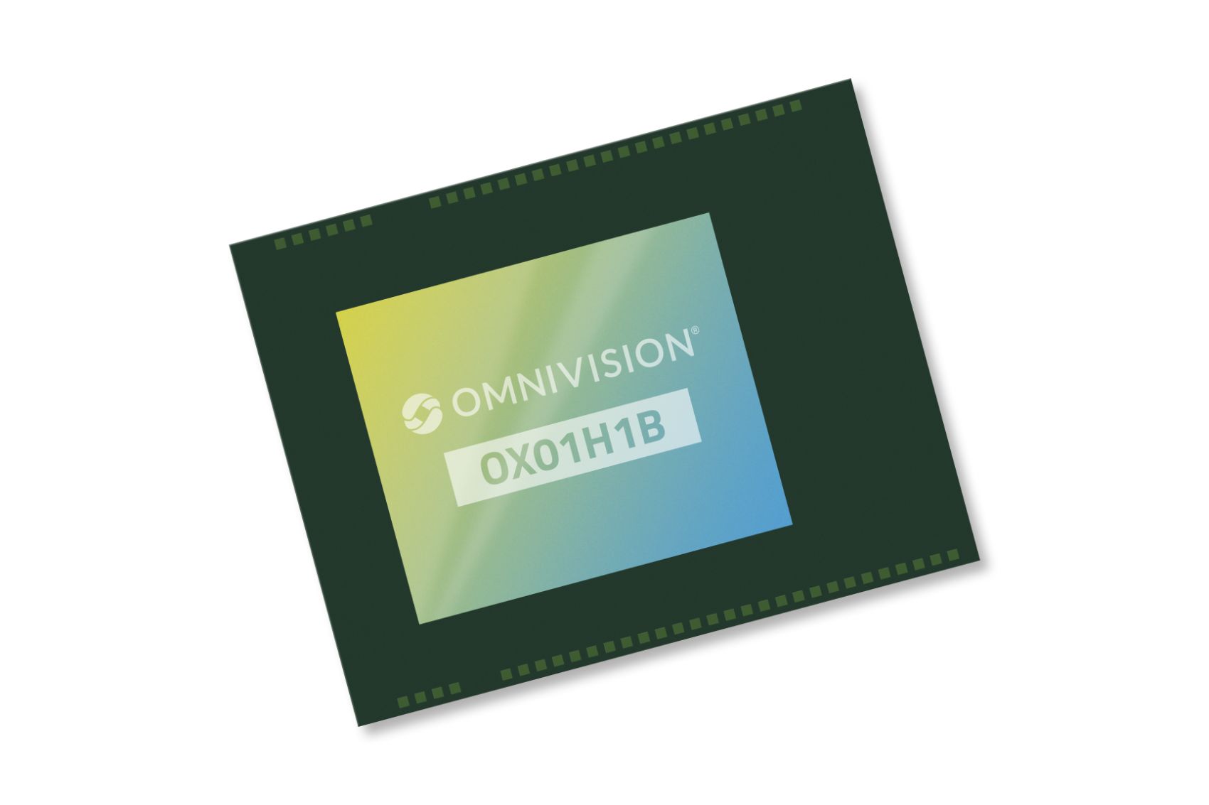
OMNIVISION has unveiled the OX02C1S and OX01H1B as the latest additions to its Nyxel near-infrared (NIR) technology family. Hallmarks of both sensors include a small 2.2-micron pixel, NIR quantum efficiency (QE) at 36 percent, and low power consumption for driver and occupant monitoring applications. News of the OX02C1S and OX01H1B follows the announcement of the OX01E20 automotive SoC for 360-degree and rearview camera systems, the latter of which is in mass production as of June 2023.
“As the automotive industry rapidly mandates advanced in-cabin sensing applications to increase driver and passenger safety, OMNIVISION is expanding its product portfolio to provide automotive OEMs with more options and flexibility in their designs,” said Paul Wu, automotive product marketing manager at OMNIVISION. “Our OX02C1S and OX01H1B sensors are the newest additions to our in-cabin solutions portfolio, with the same features as the five-megapixel OX05B1S GS sensor we introduced during the Consumer Electronics Show in 2022.”
OX02C1S & OX01H1B: Similarities & Differences
As described by Wu, the OX02C1S and OX01H1B share the same pixel technology as the existing OXO5B1S to help automotive OEMs more seamlessly incorporate any combination of them as solutions across their entire vehicle lineup. Complimenting the 2.2-micron pixel and optimum QE for increased low-light performance is a significant increase in modulation transfer function (MTF) over the previous 3.0 µm FSI GS pixel design.
Both the OX02C1S and OX01H1B utilize OmniPixel4-GS technology, enabling simultaneous image detection in all pixels to accurately reproduce rapid motion without deformation. Similarly, both sensors have integrated ASIL-B and cybersecurity measures that meet the latest industry standards.
“The OX02C1S is essentially a more economical and lower resolution (2.5MP) version of the OX05B1S for DMS and OMS, while the OX01H1B is a flexible 1.5MP solution for DMS that offers the ideal price and performance for OEMs that need the flexibility to place the DMS camera into different locations within the vehicle based on their unique interior design,” Wu said.


Reconstructed Wafer Option
In a press release highlighting the announcement, OMNIVISION noted the benefits of a stacked a-CSP package, allowing for higher-performance image sensors in tighter camera spaces and the ability for OEMs to customize their packages via a reconstructed wafer option (the stacked a-CSP package and the importance of smaller form factors was a topic of discussion with OMNIVISION on an episode of AutoVision News Radio). The OX02C1S sensor features a 2.5MP resolution in a 1/3.55-inch optical format, while the OX01H1B features a 1.5MP resolution in a 1/4.51-inch optical format.
“The CMOS image sensor market for automotive DMS and OMS can be divided into three distinct segments: digital cockpit, automated driving, and NCAP/GSR (New Car Assessment Program/General Safety Regulation) compliance. Performance requirements differ significantly for each,” explained Colin Barnden, principal analyst at Semicast Research, noting how designers must also consider the sensor’s location in the vehicle. “With the new OX02C1S and OX01H1B sensors, and existing OX05B1S, OMNIVISION provides automakers with solutions for the total market.”


